- 您现在的位置:买卖IC网 > Sheet目录486 > NTD23N03R-1G (ON Semiconductor)MOSFET N-CH 25V 3.8A IPAK
�� �
�
�NTD23N03R�
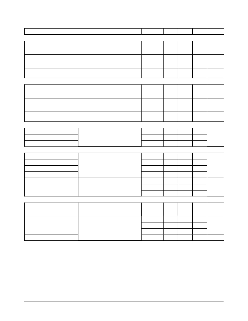
�ELECTRICAL� CHARACTERISTICS� (T� J� =� 25� °� C� unless� otherwise� specified)�
�Characteristics�
�Symbol�
�Min�
�Typ�
�Max�
�Unit�
�OFF� CHARACTERISTICS�
�Drain� ?� to� ?� Source� Breakdown� Voltage� (Note� 3)�
�(V� GS� =� 0� Vdc,� I� D� =� 250� m� Adc)�
�Temperature� Coefficient� (Positive)�
�Zero� Gate� Voltage� Drain� Current�
�(V� DS� =� 20� Vdc,� V� GS� =� 0� Vdc)�
�(V� DS� =� 20� Vdc,� V� GS� =� 0� Vdc,� T� J� =� 150� °� C)�
�Gate� ?� Body� Leakage� Current�
�(V� GS� =� ±� 20� Vdc,� V� DS� =� 0� Vdc)�
�V(br)� DSS�
�I� DSS�
�I� GSS�
�25�
�?�
�?�
�?�
�?�
�28�
�?�
�?�
�?�
�?�
�?�
�?�
�1.0�
�10�
�±� 100�
�Vdc�
�mV/� °� C�
�m� Adc�
�nAdc�
�ON� CHARACTERISTICS� (Note� 3)�
�Gate� Threshold� Voltage� (Note� 3)�
�(V� DS� =� V� GS� ,� I� D� =� 250� m� Adc)�
�Threshold� Temperature� Coefficient� (Negative)�
�Static� Drain� ?� to� ?� Source� On� ?� Resistance� (Note� 3)�
�(V� GS� =� 4.5� Vdc,� I� D� =� 6� Adc)�
�(V� GS� =� 10� Vdc,� I� D� =� 6� Adc)�
�Forward� Transconductance� (Note� 3)�
�(V� DS� =� 10� Vdc,� I� D� =� 6� Adc)�
�V� GS(th)�
�R� DS(on)�
�g� FS�
�1.0�
�?�
�?�
�?�
�?�
�1.8�
�?�
�50.3�
�32.3�
�13�
�2.0�
�?�
�60�
�45�
�?�
�Vdc�
�mV/� °� C�
�m� W�
�Mhos�
�DYNAMIC� CHARACTERISTICS�
�Input� Capacitance�
�C� iss�
�?�
�225�
�?�
�pF�
�Output� Capacitance�
�Transfer� Capacitance�
�(V� DS� =� 20� Vdc,� V� GS� =� 0� V,� f� =� 1� MHz)�
�C� oss�
�C� rss�
�?�
�?�
�108�
�48�
�?�
�?�
�SWITCHING� CHARACTERISTICS� (Note� 4)�
�Turn� ?� On� Delay� Time�
�t� d(on)�
�?�
�2.0�
�?�
�ns�
�Rise� Time�
�Turn� ?� Off� Delay� Time�
�Fall� Time�
�(V� GS� =� 10� Vdc,� V� DD� =� 10� Vdc,�
�I� D� =� 6� Adc,� R� G� =� 3� W� )�
�t� r�
�t� d(off)�
�t� f�
�?�
�?�
�?�
�14.9�
�9.9�
�2.0�
�?�
�?�
�?�
�Gate� Charge�
�(V� GS� =� 4.5� Vdc,� I� D� =� 6� Adc,�
�V� DS� =� 10� Vdc)� (Note� 3)�
�Q� T�
�Q� 1�
�Q� 2�
�?�
�?�
�?�
�3.76�
�1.7�
�1.6�
�?�
�?�
�?�
�nC�
�SOURCE� ?� DRAIN� DIODE� CHARACTERISTICS�
�Forward� On� ?� Voltage�
�Reverse� Recovery� Time�
�Reverse� Recovery� Stored� Charge�
�(I� S� =� 6� Adc,� V� GS� =� 0� Vdc)� (Note� 3)�
�(I� S� =� 6� Adc,� V� GS� =� 0� Vdc,� T� J� =� 125� °� C)�
�(I� S� =� 6� Adc,� V� GS� =� 0� Vdc,�
�dI� S� /dt� =� 100� A/� m� s)� (Note� 3)�
�V� SD�
�t� rr�
�t� a�
�t� b�
�Q� RR�
�?�
�?�
�?�
�?�
�?�
�?�
�0.87�
�0.74�
�8.7�
�5.2�
�3.5�
�0.003�
�1.2�
�?�
�?�
�?�
�?�
�?�
�Vdc�
�ns�
�m� C�
�3.� Pulse� Test:� Pulse� Width� ≤� 300� m� s,� Duty� Cycle� ≤� 2%.�
�4.� Switching� characteristics� are� independent� of� operating� junction� temperatures.�
�http://onsemi.com�
�2�
�发布紧急采购,3分钟左右您将得到回复。
相关PDF资料
NTD24N06-001
MOSFET N-CH 60V 24A IPAK
NTD24N06LG
MOSFET N-CH 60V 24A DPAK
NTD25P03L1G
MOSFET P-CH 30V 25A IPAK3
NTD2955PT4G
MOSFET P-CH 60V 12A DPAK
NTD3055-094G
MOSFET N-CH 60V 12A DPAK
NTD3055-150T4
MOSFET N-CH 60V 9A DPAK
NTD3055L104
MOSFET N-CH 60V 12A DPAK
NTD3055L170-001
MOSFET N-CH 60V 9A IPAK
相关代理商/技术参数
NTD23N03RG
功能描述:MOSFET 25V 23A N-Channel RoHS:否 制造商:STMicroelectronics 晶体管极性:N-Channel 汲极/源极击穿电压:650 V 闸/源击穿电压:25 V 漏极连续电流:130 A 电阻汲极/源极 RDS(导通):0.014 Ohms 配置:Single 最大工作温度: 安装风格:Through Hole 封装 / 箱体:Max247 封装:Tube
NTD23N03RT4
功能描述:MOSFET 25V 23A N-Channel RoHS:否 制造商:STMicroelectronics 晶体管极性:N-Channel 汲极/源极击穿电压:650 V 闸/源击穿电压:25 V 漏极连续电流:130 A 电阻汲极/源极 RDS(导通):0.014 Ohms 配置:Single 最大工作温度: 安装风格:Through Hole 封装 / 箱体:Max247 封装:Tube
NTD23N03RT4G
功能描述:MOSFET 25V 23A N-Channel RoHS:否 制造商:STMicroelectronics 晶体管极性:N-Channel 汲极/源极击穿电压:650 V 闸/源击穿电压:25 V 漏极连续电流:130 A 电阻汲极/源极 RDS(导通):0.014 Ohms 配置:Single 最大工作温度: 安装风格:Through Hole 封装 / 箱体:Max247 封装:Tube
NTD2405
功能描述:RELAY SSR AC OUT 240VAC 5A PNL RoHS:是 类别:继电器 >> 固态 系列:NTD 其它有关文件:AQx REACH Cert of Compliance 特色产品:AQY Series Relays 标准包装:1 系列:PhotoMOS™ AQY 电路:SPST-NO(1 Form A) 输出类型:AC,DC(RF) 导通状态电阻:1.25 欧姆 负载电流:250mA 输入电压:1.3VDC 电压 - 负载:0 ~ 40 V 安装类型:表面贴装 端接类型:SMD(SMT)接片 封装/外壳:4-SMD(0.175",4.45mm) 供应商设备封装:4-SSOP 包装:Digi-Reel® 继电器类型:继电器 其它名称:255-2683-6
NTD24061
制造商:ONSEMI 制造商全称:ON Semiconductor 功能描述:Power MOSFET 60 Volt, 24 Amp Na??Channel DPAK
NTD2406-1
制造商:ONSEMI 制造商全称:ON Semiconductor 功能描述:Power MOSFET 60 V, 24 A, N-Channel DPAK
NTD24061G
制造商:ONSEMI 制造商全称:ON Semiconductor 功能描述:Power MOSFET 60 Volt, 24 Amp Na??Channel DPAK
NTD2410
功能描述:固态继电器-工业安装 10A TRIAC OUTPUT
RoHS:否 制造商:Crydom 控制电压范围:4 VDC to 32 VDC 负载电压额定值:7 VDC to 72 VDC 负载电流额定值:160 A 触点形式: 输出设备:SSR 安装风格:Panel